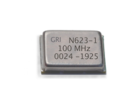
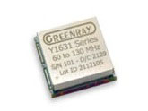
| Items |
 N623 Low Phase Noise Low G-Sensitivity Oscillator |
 Y1600 Compact Rugged Package Good Phase Noise Performance Oscillator |
 Y1631 Low Phase Noise Ultra-Low G-Sensitivity Oscillator |
|||
| Description | Greenray Industries' N623 VCXO offers ultra-low phase noise and low g-sensitivity performance in a compact, SMD package. | Greenray Industries' Y1600 XO offers good phase noise performance in a compact, rugged package | Greenray Industries' Y1631 XO offers good phase noise performance in a compact, rugged package | |||
| Rugged DIP Package | 20.3 x 12.7 mm | 20.3 x 12.7 mm | ||||
| Direct Current (DC) Supply Voltage | 5 V | 5 V | ||||
| Package Size | 17.3 mm² | |||||
| Frequency Range | 10 to 100 MHz | 60 to 130 MHz | ||||
| Surface Mount Device (SMD) Package Width | 9.1 mm | |||||
| Surface Mount Device (SMD) Package Length | 14.2 mm | |||||
| Frequency (Other Frequencies and Options Available) | 100 MHz | |||||
| Typical Nominal Frequency at 25 Degrees Celsius (ºC) Temperature Set Point | 100 MHz | |||||
| Minimum Nominal Frequency at High Speed Complementary Metal-Oxide-Semiconductor (HCMOS) | 10 MHz | |||||
| Maximum Nominal Frequency at High Speed Complementary Metal-Oxide-Semiconductor (HCMOS) | 100 MHz | |||||
| Minimum Nominal Frequency at Sinewave | 60 MHz | |||||
| Maximum Nominal Frequency at Sinewave | 130 MHz | |||||
| Typical Frequency Stability (±) at -40 to +85 Degrees (ºC) Temperature Set Point | 15 ppm | |||||
| Typical Frequency Stability (±) at 0 to +50 Degrees Celsius (ºC) Temperature | 5 ppm | |||||
| Typical Frequency Stability (±) at -20 to +70 Degrees Celsius (ºC) Temperature (N106) | 10 ppm | |||||
| Typical Frequency Stability (±) at -20 to +70 Degrees Celsius (ºC) Temperature | 15 ppm | |||||
| Typical Frequency Stability (±) at -40 to +85 Degrees Celsius (ºC) Temperature | 15 ppm | 20 ppm | ||||
| Note for Frequency Stability | Other Stability Available | Other Stability Available | ||||
| Maximum Aging Tolerance (±) for 1 Year | 1.0 ppm | |||||
| Maximum Aging (±) at 10 years (10 Megahertz (MHz)) | 3 ppm | |||||
| Maximum Aging (±)at 10 years (100 Megahertz (MHz)) | 3 ppm | |||||
| Maximum Acceleration Sensitivity1 | 2.5 ppb/g | |||||
| Maximum Acceleration Sensitivity (SD) | 2.0 ppb/g | |||||
| Maximum Acceleration Sensitivity (LG) | 0.5 ppb/g | |||||
| Maximum Acceleration Sensitivity (ULG) | 0.09 ppb/g | |||||
| Note for Acceleration Sensitivity | Acceleration Sensitivity is worst axis tested at 90 Hz, 10 g | Acceleration Sensitivity is worst axis tested at 90 Hz, 10 g | ||||
| Maximum Frequency Versus Voltage for a 5 Percent (%) Change (±) | 0.1 ppm | 0.1 ppm | ||||
| Maximum Frequency Versus Load for a 10% Change (±) | 0.1 ppm | 0.1 ppm | ||||
| Typical Electronic Frequency Control (EFC) (0 to Voltage Drain to Drain (VDD) - 0.5 Positive Slope) (±) | 30 ppm | 10 ppm | ||||
| Typical Electronic Frequency Control (EFC) (0.5 to Voltage Drain to Drain (VDD) - 0.5 Positive Slope) (±) | 10 ppm | |||||
| Maximum Electronic Frequency Control (EFC) Linearity (0.5 to Voltage Drain to Drain (VDD) - 0.5) | 10 % | |||||
| Minimum Absolute Pull Range at All Condition 7 Years | -10 ppm | |||||
| Maximum Absolute Pull Range at All Condition 7 Years | 10 ppm | |||||
| Typical Frequency Versus Voltage (±) at ± 0.25 Voltage (V) | 1 ppm | |||||
| Typical Phase Noise at 100 Megahertz (MHz) Static Nominal Frequency and 10 Hertz (Hz) Frequency Offset | -85 dBc/Hz | |||||
| Typical Phase Noise at 100 Megahertz (MHz) Static Nominal Frequency and 100 Hertz (Hz) Frequency Offset | -115 dBc/Hz | |||||
| Typical Phase Noise at 100 Megahertz (MHz) Static Nominal Frequency and 1000 Hertz (Hz) Frequency Offset | -140 dBc/Hz | |||||
| Typical Phase Noise at 100 Megahertz (MHz) Static Nominal Frequency and 10000 Hertz (Hz) Frequency Offset | -162 dBc/Hz | |||||
| Typical Phase Noise at 100 Megahertz (MHz) Static Nominal Frequency and 100000 Hertz (Hz) Frequency Offset | -173 dBc/Hz | |||||
| Typical Phase Noise at 100 Megahertz (MHz) Static Nominal Frequency and 1000000 Hertz (Hz) Frequency Offset | -175 dBc/Hz | |||||
| Typical Phase Noise at 10 Megahertz (MHz) Static Nominal Frequency and 10 Hertz (Hz) Frequency Offset | -105 dBc/Hz | -83 dBc/Hz | ||||
| Typical Phase Noise at 10 Megahertz (MHz) Static Nominal Frequency and 100 Hertz (Hz) Frequency Offset | -135 dBc/Hz | -120 dBc/Hz | ||||
| Typical Phase Noise at 10 Megahertz (MHz) Static Nominal Frequency and 1000 Hertz (Hz) Frequency Offset | -155 dBc/Hz | -149 dBc/Hz | ||||
| Typical Phase Noise at 10 Megahertz (MHz) Static Nominal Frequency and 10000 Hertz (Hz) Frequency Offset | -160 dBc/Hz | -160 dBc/Hz | ||||
| Typical Phase Noise at 10 Megahertz (MHz) Static Nominal Frequency and 100000 Hertz (Hz) Frequency Offset | -162 dBc/Hz | -167 dBc/Hz | ||||
| Typical Phase Noise at 10 Megahertz (MHz) Static Nominal Frequency and 1000000 Hertz (Hz) Frequency Offset | -170 dBc/Hz | |||||
| Maximum Phase Noise at 100 Megahertz (MHz) Static Nominal Frequency and 10 Hertz (Hz) Frequency Offset | -80 dBc/Hz | |||||
| Maximum Phase Noise at 100 Megahertz (MHz) Static Nominal Frequency and 100 Hertz (Hz) Frequency Offset | -110 dBc/Hz | |||||
| Maximum Phase Noise at 100 Megahertz (MHz) Static Nominal Frequency and 1000 Hertz (Hz) Frequency Offset | -135 dBc/Hz | |||||
| Maximum Phase Noise at 100 Megahertz (MHz) Static Nominal Frequency and 10000 Hertz (Hz) Frequency Offset | -158 dBc/Hz | |||||
| Maximum Phase Noise at 100 Megahertz (MHz) Static Nominal Frequency and 100000 Hertz (Hz) Frequency Offset | -170 dBc/Hz | |||||
| Maximum Phase Noise at 100 Megahertz (MHz) Static Nominal Frequency and 1000000 Hertz (Hz) Frequency Offset | -173 dBc/Hz | |||||
| Minimum Direct Current (DC) Supply Voltage Drain to Drain (VDD) | 4.75 V | |||||
| Typical Direct Current (DC) Supply Voltage Drain to Drain (VDD) | 5.0 V | |||||
| Maximum Direct Current (DC) Supply Voltage Drain to Drain (VDD) | 5.25 V | |||||
| Typical Supply Current at 100 Megahertz (MHz) Frequency | 30 mA | |||||
| Maximum Supply Current at 100 Megahertz (MHz) Frequency | 50 mA | |||||
| Maximum Supply Current at 10 Megahertz (MHz) Frequency | 15 mA | |||||
| Typical Load | 50 Ohms | 50 Ohms | ||||
| Minimum Load at Complementary Metal-Oxide-Semiconductor (CMOS) | 10 pF | |||||
| Typical Load at Complementary Metal-Oxide-Semiconductor (CMOS) | 15 pF | |||||
| Minimum Level 50 O Load | 10 dBM | |||||
| Minimum Power Level at 25 Degrees Celsius (ºC) Temperature | +9.5 dBM | |||||
| Typical Power Level at 25 Degrees Celsius (ºC) Temperature | +12 dBM | |||||
| Maximum Power Level at 25 Degrees Celsius (ºC) Temperature | +14.5 dBM | |||||
| Minimum Level (1) 15 Power Factor (pF) Load, 5.0 Volts (V) | +4.5 V | |||||
| Maximum Level (0) 15 Power Factor (pF) Load, 5.0 Volts (V) | +0.2 V | |||||
| Minimum Symmetry at Complementary Metal-Oxide-Semiconductor (CMOS) | 45 % | |||||
| Typical Symmetry at Complementary Metal-Oxide-Semiconductor (CMOS) | 50 % | |||||
| Maximum Symmetry at Complementary Metal-Oxide-Semiconductor (CMOS) | 55 % | |||||
| Maximum Supply Current | 30 mA | |||||
| Maximum Harmonics | -30 dBc | -45 dBc | ||||
| Maximum Spurious | -90 dBc | |||||
| Random Vibration |
Standard MIL-STD-202 Method, Condition 214, Cond I-A Description 0.2 PSD, 5.35 rms G |
Standard MIL-STD-202 Method, Condition 214, Cond I-A Description 0.3 PSD, 20.7 G rms |
||||
| Vibration |
Standard MIL-STD-202 Method, Condition Method 204, Condition Cond A Description 10 g peak, 10 and 500 Hz |
|||||
| Sine Vibration |
Standard MIL-STD-202 Method, Condition 204, Cond D Description 20 g, 20 to 2,000 Hz |
|||||
| Shock |
Standard MIL-STD-202 Method, Condition Method 213, Condition Cond C Description 100 g, 6 ms half-sine, 12.3 ft/sec |
Standard MIL-STD-202 Method, Condition 213, Cond C Description 100 g, 6 ms half-sine |
Standard MIL-STD-202 Method, Condition 213, Cond C Description 30 g, 11 ms, sawtooth |
|||
| Operating Temperature | -40 to +85 ºC | |||||
| Storage Temperature | -45 to +95 ºC | -55 to +85 ºC | -55 to +85 ºC | |||
| Terminal Finish | Gold plating (RoHS) is standard (E). SnPb 63/37 also available | |||||
| Package Weight | 3 g | 3 g | <3 g | |||
| Soldering Instruction | Reflow Solder | Hand | Hand Reflow Soldering | |||
| Shipping | Tray | Tray | Tray Pack | |||
| Marking |
Line 1: Greenray logo + Model Line 2: Frequency Line 3: Serial number + Data code (YYWW) |
Line 1: Greenray logo + Model Line 2: Frequency Line 3: Serial Number + Data Code (YYWW) |
Line 1: Greenray logo Line 2: Model Line 3: Frequency Line 4: Serial Number + Data Code (YYWW) Line 5: Lot Number |
|||
| Applications |
|
|
|
|||
| Features |
|
|
|
|||
|
||||||